UNIST UNIST

ADMISSIONS

발전기금 알림마당
모바일메뉴 열기
 

UNIST site map

전체 메뉴 닫기
STUDENT
 
Scroll Down

UNIST Today

we are all

pioneers!

UNIque & beST

Nexus

UNIST Today

we are all

pioneers!

UNIque & beST

Nexus

Information for UNISTar

WHY UNIST

star

Global
Campus for
Future
Innovators

Research AREA

중점연구분야

Research
AREA

에너지·AI·미래산업에 집중하다

UNIST는 에너지 전환, AI, 미래산업이라는
대한민국의 핵심 과제에 연구 역량을 집중합니다.

  • 에너지 전환
  • 이차전지 · 수소 · 탄소중립
  • Ai 기반 산업 혁신
  • 반도체 · 소재 · 양자
EDUCATION INNOVATION

교육혁신프로그램

EDUCATION
INNOVATION

이론을 배우는 것을 넘어 직접
연구하며 성장하다

UNIST의 학부생부터 대학원생까지 연구의
보조가 아닌 주체로 성장하는 경험을 제공합니다.

  • 학부생 연구참여
  • 국제학회·논문참여
  • 소수정예 밀착 연구지도
industry collaboration

산학협력

industry
collaboration

연구에서 산업까지, 현장과 가장
가까운 UNIST

대한민국 최대 산업도시 울산에 위치한
UNIST는 연구 성과가 기업과 산업 현장으로
가장 빠르게 연결되는 구조를 갖추고 있습니다.

  • 기술사업화·창업지원
  • 울산 산업단지
  • 대기업 · 공기업과의 공동연구
Research support

연구지원

Research
support

젊은 UNIST, 연구에 최적화된
유연한 캠퍼스

UNIST는 가장 늦게 출범한 과기원으로,
관행에 얽매이지 않는 유연한 연구·교육 시스템을
갖추고 있습니다.

  • 빠른 신흥 분야 대흥
  • 단일 캠퍼스 기반
  • 생활.연구 일체형 구조
  • 개방형 연구 공간

Research Impact

star

근적외선 ‘좌우 회전 빛’ 읽어내는 고성능 광검출기 개발

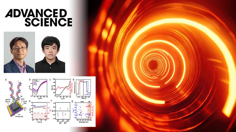
적외선 빛의 원편광 성분을 검출하는 고성능 광검출기가 개발됐다. 사물의 형태 뿐만 아니라 재질 차이까지 구분할 수 있는 자율주행 센서, DNA·단백질 같은 생체 분자를 관찰하는 바이오이미징 기술 개발 등에 도움이 될 것으로 기대된다. UNIST 화학과 김봉수 교수와 서울대학교 오준학 교수팀은 키랄 유기반도체 박막 물질을 수직형 트랜지스터 구조에 적용한 고성능 근적외선 원평광 검출기를 개발했다고 23일 밝혔다. 원편광 검출기는 사물의 형태와 재질을 구분하는 자율주행 센서나 생체분자 관찰, 보안 기술 등에 쓸 수 있는 광센서다. 빛이 왼쪽으로 회전하는 좌원편광인지 오른쪽으로 회전하는 우원편광인지를 검출하는 것으로, 빛의 회전 방향에 따라 발생하는 전류의 크기를 읽어내는 방식으로 작동한다. 개발된 광검출기는 850나노미터 근적외선에서 원편광 구분 능력을 나타내는 광전류 비대칭 지수 0.1을 기록했다. 비대칭 지수가 높을수록 좌우 편광을 잘 구분할 수 있다. 미세한 빛을 잡음과 구별하는 비검출도는 4.9×10¹¹ 존스, 외부양자효율은 최대 909%였으며, 빛에 반응하는 시간도 600마이크로초 이내였다. 이는 기존 근적외선 원편광 검출기 가운데 최고 수준의 성능이다. 이 같은 고성능의 원인 중 하나는 검출기 안에 들어 있는 키랄 분자 박막을 열처리했기 때문이다. 키랄 분자는 구조의 좌우 대칭이 깨진 특수 분자로, 좌원편광과 우원편광의 흡수율이 달라 별도의 편광 광학부품 없이 빛의 회전 방향을 직접 구분할 수 있다. 하지만 일반적으로 키랄 분자를 박막 형태로 만들면 비대칭적인 구조 탓에 분자들이 차곡차곡 정렬되지 않아 검출 성능이 저하되는데, 연구팀은 분자 끝에 불소가 달린 키랄 분자 박막을 열처리해 원편광을 구분하는 성능을 높였다. 열처리는 박막 속 분자들을 더 크고 규칙적인 결정 구조로 재배열하는 것으로 나타났다. 실제 불소 치환 박막의 원편광 흡수 선택성은 열처리 전 약 0.03에서 250℃ 열처리 후 약 0.1로 3배 이상 높아졌다. 박막 속 분자 배열을 분석해 보니, 열처리한 박막에서는 분자들이 단결정처럼 규칙적으로 정돈돼 있었다. 실제 단결정의 배열과 비교했을 때도 주요 특징이 일치했다. 열처리 후에는 박막이 더 잘 흡수하고 검출하는 원편광의 방향도 반대로 바뀌었다. 열을 받은 분자들이 다른 적층 구조로 다시 쌓이면서 박막 전체의 나선 배열 방향이 뒤집혔기 때문이다. 반면 분자 끝에 염소가 달린 박막은 약 150℃ 이후에는 구조 변화가 거의 나타나지 않았으며, 열처리 후 원편광 흡수 선택성도 오히려 낮아졌다. 연구팀은 좌원편광과 우원편광의 흡수 차이로 생긴 전류 차이를 증폭할 수 있도록, 이 박막을 수직형 트랜지스터에 적용했다. 수직형 트랜지스터는 수평형보다 전하 이동 거리가 짧고 분자가 쌓인 방향과 전류가 흐르는 방향이 맞아 빛으로 생긴 전하를 빠르게 모으고 증폭할 수 있다. 공동연구팀은 “분자 말단의 원자 종류와 열처리 온도가 박막의 분자 배열과 원편광 선택성을 어떻게 바꾸는지를 규명해, 고성능 키랄 광전자소자를 만들기 위한 박막 후처리 기준을 제시했다”며 “자율주행용 근적외선 센서와 바이오이미징 등 편광 정보를 정밀하게 읽는 기술에 활용할 수 있을 것”이라고 설명했다. 이번 연구는 과학기술정보통신부 한국연구재단(NRF)의 지원을 받아 수행됐으며, 연구 결과는 세계적인 학술지인 어드밴스드 사이언스 (Advanced Science)에 6월 28일 온라인 공개됐다.

2026.08.10

  • 광검출기
  • 광센서
  • 근적외선
  • 바이오센서
  • 수직트랜지스터
  • 자율주행
  • 카이랄분자
  • 키랄분자
  • 화학과

“지웠는데 되살아나는 AI의 기억 막는다”.. 머신 언러닝 기술 개발

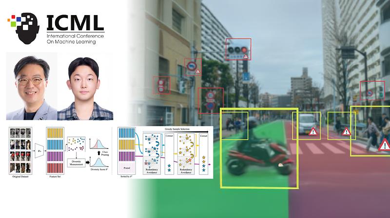
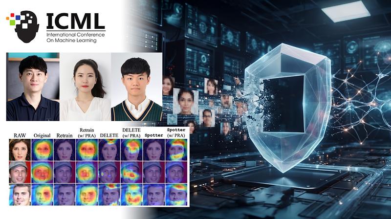
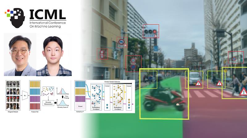
인공지능(AI)이 학습한 민감 개인정보나 저작권 위반 데이터를 지울 때 정상 정보는 보존하면서 삭제한 정보가 다시 살아나는 것은 막는 ‘기억 지우개’ 기술이 새롭게 개발됐다. UNIST 인공지능대학원 윤성환 교수팀과 산업공학과 박새롬 교수팀은 지워야 할 정보와 닮은 정상 정보는 보호하고, 삭제 대상 사진 몇 장만으로 인식 능력을 되살리는 공격까지 막는 ‘머신 언러닝 기술’인 ‘스포터(Spotter)’를 개발했다고 21일 밝혔다. 머신 언러닝(Machine Unlearning)은 학습을 마친 AI에서 특정 데이터나 범주가 미친 영향만 선택적으로 없애는 기술이다. 얼굴 인식 AI에서 삭제를 요청한 사람의 얼굴 정보를 지우거나, 학습 데이터에 포함된 개인정보와 유해 콘텐츠를 제거하는 데 쓸 수 있다. 스포터는 삭제 대상과 비슷한 정상 정보를 구별하는 AI의 능력은 그대로 유지하면서, 삭제 대상 사진들에서 공통점을 찾아내는 능력은 없애는 기술이다. 덕분에 지우지 않아야 할 정보의 인식 성능을 보호하고, 공격자가 삭제 대상 사진 몇 장을 확보하더라도 지워진 인식 기준을 다시 만들기 어렵다. 연구팀은 기존 언러닝 기술의 약점인 ‘과잉 삭제’와 ‘삭제한 정보가 다시 살아날 수 있는 재학습 취약성’을 자체 실험으로 진단해 이 같은 기술을 개발했다. 기존 언러닝 기술로 AI가 특정 범주를 더 이상 인식하지 못하도록 한 결과, 전체 평균 정확도는 높게 유지됐지만 삭제 대상과 닮은 정상 정보의 인식 성능은 떨어지는 것으로 나타났다. 또 삭제 대상의 특징이 AI 안에 남아 있어, 관련 사진 몇 장만 다시 보여줘도 지웠던 인식 능력이 되살아날 수 있었다. 예를 들어 ‘고양이’를 삭제했다면, 이와 유사한 호랑이나 표범의 인식 정확도가 떨어질 수 있고, 고양이를 인식하는 데 필요했던 개별 정보가 식별 가능한 군집 형태로 남아 있어 고양이 사진 몇 장만 다시 넣어주면 고양이를 판별하는 능력을 되살릴 수 있는 것이다. 제1저자인 하승범 연구원은 “기존에는 AI가 삭제 대상을 더 이상 알아보지 못하는지와, 삭제하지 않은 나머지 정보의 전체 평균 인식 성능이 유지되는지만 주로 평가했기 때문에 삭제 대상과 닮은 일부 정보를 인식하는 성능 저하나, 지운 정보가 다시 살아나는 것과 같은 사각지대가 잘 드러나지 않았었다”라고 설명했다. CIFAR-10 데이터셋으로 실험한 결과, 스포터는 삭제 대상의 인식 정확도를 0%로 낮췄으며, 재학습 공격 뒤에도 인식 정확도를 0.24%로 억제할 수 있었다. 반면 기존 언러닝 기술은 사진 5장을 이용한 재학습 공격 뒤 삭제 대상에 대한 인식 정확도가 71.10%에서 최대 99.98%까지 되살아났다. 또 스포터는 삭제하지 않은 나머지 범주에 대해 인식 정확도 99.96%를 유지했다. 소형 이미지 데이터셋인 CIFAR-10뿐만 아니라, 더 큰 이미지 데이터셋인 타이니이미지넷과 실제 얼굴 인식 데이터셋인 CASIA-WebFace에서도 유사한 성능을 확인했다. 공동 연구팀은 “언러닝 기술의 사각지대를 보완하기 위해 개발된 스포터는 기존 언러닝 기법에 쉽게 결합할 수 있는 플러그인(plug-and-play) 형태로 설계돼 얼굴 인식과 유해 콘텐츠 삭제 등 개인정보 보호가 중요한 AI 서비스에 두루 활용될 수 있을 것”이라고 기대했다. 이번 연구는 인공지능 분야 세계 최고 권위의 국제학술대회인 국제머신러닝학회(International Conference on Machine Learning, ICML)에 채택됐다. 2026 ICML은 지난 7월 6일부터 11일까지 서울에서 열렸다. 연구 수행은 과기정통부・한국연구재단(NRF)의 지원을 받는 ‘중견연구사업’과 과기정통부・정보통신기획평가원의 지원을 받는 ‘초거대산업AI연구지원(R&D)사업’, ‘인공지능대학원지원사업’, ‘AI 스타펠로우십사업’, ‘지역지능화혁신인재양성사업’, ‘대학ICT연구센터사업’의 지원을 받아 수행되었다.

2026.08.06

  • 개인정보
  • 머신러닝
  • 머신언러닝기술
  • 보안기술
  • 산업공학과
  • 인공지능대학원
  • 인물사진
  • 재학습공격

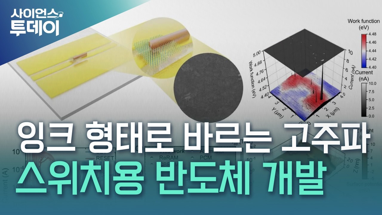
반도체 잉크 발라 6G·우주통신용 고주파 스위치 만든다!

잉크 상태의 원료를 기판에 발라 만든 이차원 반도체 박막을 기반으로 하는 통신용 반도체 소자가 새롭게 개발됐다. UNIST 전기전자공학과 김명수 교수팀은 용액공정으로 만든 이황화몰리브덴(MoS₂) 박막을 이용해 67기가헤르츠(GHz) 대역까지 작동하는 저전력·고성능 고주파 스위치를 개발했다고 22일 밝혔다. RF(고주파) 스위치는 스마트폰, 위성통신, 레이더, 무선기지국, 자율주행 통신 장비 등에서 고주파 신호의 흐름을 연결하거나 차단하는 필수 반도체 소자다. 특히 6G와 우주통신처럼 많은 안테나와 주파수 채널을 동시에 사용하는 시스템에서는 낮은 삽입손실과 높은 절연 성능, 낮은 소비전력의 3박자를 갖춘 스위치가 필요하다. 연구팀이 개발한 스위치는 병렬형 구조에서 67GHz 기준 삽입손실 0.1데시벨(dB) 미만, 절연도 35dB 이상의 성능을 기록했다.1초에 670억 번 진동하는 고주파 신호가 들어왔을 때 입력 신호의 약 98%를 거의 손실 없이 통과시키고, 스위치를 껐을 때 새는 신호는 0.03% 이하로 억제했다는 의미다. 일반적으로 주파수가 높아질수록 신호 손실과 누설이 커지기 쉬운데, 6G와 위성통신에 쓰이는 밀리미터파 대역에서도 낮은 삽입손실과 높은 절연 성능을 동시에 유지한 것이다. 신호의 통과와 차단 성능을 종합한 지표인 작동 저항과 차단 정전용량의 곱도 약 0.8펨토초로, 1펨토초보다 작은 ‘서브 펨토초급’ 성능을 달성했다. 또 스위치를 켜거나 끈 상태를 유지하기 위한 대기전력 소모도 없다. 이 스위치는 이황화몰리브덴 반도체 박막을 금속 전극 사이에 넣은 구조로, 전압을 가하면 전극에서 나온 이온이 통로를 형성하며 스위치를 켜는 방식이라, 전원을 꺼도 이미 만들어진 통로가 유지되는 덕분이다. 특히 스위치에 들어간 이황화몰리브덴 박막은 용액공정으로 만들어져 제조가 간단하고 넓은 면적에 적용하기도 쉽다. 용액공정은 반도체 소재를 액체 상태로 만든 뒤 기판에 직접 바르는 방식으로, 박막을 별도로 성장시켜 떼어 옮기는 복잡한 전사 과정이 필요 없다. 일반적으로 용액공정에서는 황 원자 자리가 비는 결함이 발생하기 쉬운데, 반도체 스위치에서는 이 황 빈자리가 구리 이온의 이동 경로를 일정하게 잡아주는 역할을 해 오히려 내구성을 향상시키는 것으로 분석됐다. 실제로 기계적으로 떼어낸 이황화몰리브덴 박막으로 만든 스위치는 반복 작동 수명이 약 100회에 그쳤지만, 용액공정 박막을 쓴 스위치는 2,000회 반복 작동에도 성능을 유지했다. 연구팀은 개발한 스위치를 실제 통신 회로에도 적용해 성능을 검증했다. 하나의 안테나를 송신기와 수신기에 번갈아 연결하는 회로와, 여러 안테나에서 나오는 전파의 타이밍을 조절해 빔의 방향을 바꾸는 위상변위기를 제작해 정상 작동을 확인했다. 위상변위기는 여러 안테나가 전파를 내보내는 시점을 조절해 빔의 방향을 바꾸는 회로로, 안테나 자체를 움직이지 않고도 전파 방향을 빠르게 바꿀 수 있어 이동 위성이나 드론처럼 위치가 계속 달라지는 대상을 빠르게 추적할 수 있다. 김명수 교수는 “복잡한 전사 공정이 필요 없는 용액공정 제조 이차원 반도체 물질로, 밀리미터파 대역에서도 신호 손실은 낮고 차단 성능은 높은 RF 스위치를 개발했다”며 “전원을 꺼도 스위치 상태가 유지돼 대기전력이 들지 않는 만큼, 6G와 위성통신, 레이더, 방산용 전파 제어 시스템을 더 작고 에너지 효율적으로 만드는 데 활용할 수 있을 것”이라고 설명했다. 이번 연구는 과학기술정보통신부 한국연구재단, 정보통신기획평가원의 우수신진연구, Space-K BIG 프로젝트, InnoCORE 사업, 지역지능화혁신인재양성사업의 지원을 받아 수행되었으며, 연구 결과는 세계적 학술지 ‘네이쳐 커뮤니케이션즈(Nature Communications)’에 6월 18일 온라인 공개됐다.

2026.08.05

  • RF스위치
  • 고주파스위치
  • 안테나
  • 우주방산
  • 위성
  • 전기전자공학과
  • 통신
  • 프론트엔드

“산화물 반도체 결함의 성질, 전체 밀도 아닌 특정 원자 간 거리가 좌우”

산화물 반도체의 성능을 좌우하는 산소 빈자리 결함의 작동 원리가 새롭게 밝혀졌다. 디스플레이·차세대 메모리용 산화물 반도체의 열처리와 박막 구조를 정하는 공정 설계의 토대가 될 전망이다. UNIST 반도체소재·부품대학원 정창욱 교수팀은 산화물 반도체의 산소 빈자리 결함의 성질을 결정하는 것은 반도체 물질 전체에 원자들이 얼마나 촘촘하게 들어차 있는지가 아니라, 결함 주변의 금속 원자 사이 거리라는 사실을 이론 계산을 통해 증명했다고 19일 밝혔다. 산화물 반도체 IGZO는 인듐, 갈륨, 아연과 산소로 이뤄진 물질이다. 낮은 온도에서 박막으로 만들기 쉬워 스마트폰과 TV 화면을 작동시키는 박막트랜지스터 반도체 소자 재료로 널리 쓰인다. 이 IGZO를 박막으로 제조하는 과정에서 산소 자리가 듬성듬성 비는 결함이 생기는데, 이 결함이 전류 흐름과 작동 전압을 바꿔 소자 성능을 불안정하게 만들 수 있다. 산소가 빠진 자리에 남은 두 개의 전자가 빈자리 주변에 갇히느냐 박막 전체로 퍼지느냐에 따라 소자의 작동 전압과 성능이 달라지는 것이다. 이번 연구에 따르면, 전자가 빈자리 주변에 갇히거나 박막 전체로 퍼지는 상태는 산소 빈자리 주변의 원자 배열에 따라 달라진다. 특정 금속 원자 사이가 가까워지면 전자가 빈자리 주변에 갇히고, 멀어지면 박막 전체로 퍼지는 것이다. 이 차이는 산소 빈자리에 남은 전자가 머무는 에너지 위치인 ‘결함 준위’의 변화에서 비롯된다는 설명이다. 결함 준위가 낮고 깊을수록 전자가 빈자리에 강하게 붙잡혀 빠져나오기 어렵다. 열처리와 박막을 잡아당기는 인장은 모두 산소 빈자리 주변의 특정 금속 원자 사이를 벌려 이 결함 준위를 높이는 효과가 있다. 결함 준위가 높아지면 전자는 빈자리에서 빠져나와 박막 전체로 퍼지기 쉬워진다. 열처리를 하면 원자들이 더 안정적인 위치로 재배열되면서 금속 이온끼리 밀어내는 에너지까지 줄어, 전자가 퍼진 상태가 에너지 측면에서 더 안정한 상태가 된다. 연구팀의 이론은 기존에 서로 맞지 않아 보였던 열처리와 압축이 각각 산소 빈자리의 성질에 미치는 영향도 일관되게 설명할 수 있다. 열처리는 산화물 반도체의 원자 배열과 전기적 특성을 조절하기 위해 쓰이는 공정이다. 기존에는 열처리하면 박막 내부의 빈 공간이 줄고 전체 원자 밀도가 높아져 산소 빈자리 주변에 갇힌 전자가 박막 전체로 퍼진다고 봤다. 하지만 박막을 압축하면 마찬가지로 밀도가 높아져도 전자가 오히려 산소 빈자리 주변에 갇히는 현상이 보고돼 왔다. 연구팀은 원자와 전자의 상태를 계산하는 밀도범함수이론과 구성좌표 분석, 열을 받은 원자들의 움직임을 시간에 따라 재현하는 제일원리 분자동역학 시뮬레이션을 통해 이 같은 사실을 밝혀냈다. 정창욱 교수는 “산소 빈자리 결함은 산화물 반도체에서 피하기 어려운 결함이지만, 그 결함의 전기적 역할을 공정 조건으로 조절할 수 있음을 이번 연구를 통해 입증했다”며 “열처리 조건이나 박막에 걸리는 응력을 설계하면 문턱전압, 전류가 켜지고 꺼지는 특성, 신뢰성을 함께 제어하는 데 활용할 수 있을 것”이라고 설명했다. 이번 연구는 미국화학회(ACS)에서 발행하는 케미스트리 오브 머티리얼즈(Chemistry of Materials)에 6월 23일 출판됐다. 연구 수행은 한국연구재단(NRF) 나노·소재기술개발사업(2710089547)의 지원을 받아 이뤄졌다.

2026.08.03

  • IGZO
  • vacancy
  • 박막반도체
  • 반도체소재부품대학원
  • 산소빈자리결함
  • 산화물반도체
  • 열처리
  • 인장

손가락 위치 묻자 '찍기' 수준으로 답하던 AI… 160만 연습문제로 손 이해력 높였다!

손은 인공지능이 인식하기 까다로운 대상 중 하나다. 한 손에 21개나 되는 관절이 촘촘히 있는 데다 각도에 따라 같은 손동작도 완전히 다르게 보이기 때문이다. 사진 속 사물은 잘 알아보는 인공지능(AI)도 손가락이 얼마나 굽었는지, 어느 관절이 앞에 있는지 같은 세밀한 손 자세는 자주 틀린다. 기존 비전 AI의 성능 평가는 사물의 종류나 상황을 묻는 데 치우쳐 이런 약점이 제대로 드러나지 않았는데, 국내 연구진이 이를 세부적으로 진단하고 부족한 능력까지 학습시킬 수 있는 표준 평가 자료를 내놨다. 로봇 조작, 증강·가상 현실, 원격 수술·재활 보조 등 정확한 사람 손동작 인식이 필요한 분야 기술 개발에 활용될 수 있을 전망이다. 인공지능대학원 백승렬 교수팀은 자신이 인식한 것을 말로 설명할 수 있는 AI 모델인 비전언어모델의 손 자세 이해력을 평가하고 학습시킬 수 있는 벤치마크 데이터셋 ‘HandVQA’를 제시했다. 벤치마크 데이터셋은 여러 AI 모델에 같은 문제를 풀게 해 성능을 객관적으로 비교하고, 어떤 유형에서 반복적으로 틀리는지를 찾아내는 표준 시험과 같다. 문제와 정답을 다시 학습시키면 부족한 능력을 보완하는 교재로도 쓸 수 있다. 연구팀은 손 사진과 21개 관절의 3차원 좌표가 함께 담긴 자료를 객관식 문제로 자동 변환하는 프로그램을 만들어, 사진 한 장당 25개씩 총 160만 개가 넘는 평가 문항을 생성했다. 프로그램은 관절 좌표에서 손가락의 굽힘 각도와 관절 사이 거리, 좌우·상하·앞뒤 위치 관계를 계산한 뒤, 이를 ‘펴짐·굽힘’, ‘가까움·벌어짐’, ‘앞·뒤’ 등으로 나눠 질문과 보기, 정답으로 바꾼다. HandVQA로 주요 비전언어모델을 평가해 본 결과, 손 자세를 따로 배우지 않은 비전언어모델들은 방향 관계를 묻는 문제에서 거의 ‘찍기’와 비슷한 수준의 정확도를 보였다. 특히 관절 사이 거리를 판단하는 데 어려움을 겪었다. 비전언어모델인 ‘라바(LLaVA)’를 HandVQA 데이터셋으로 미세조정해 학습시키자, 관절 거리 판단 정확도가 기존 16.20%에서 90.79%로 대폭 향상됐다. 또 다른 비전언어모델인 큐웬(Qwen)은 HandVQA로 학습한 뒤 손동작 인식과 손·물체 상호작용 과제를 별도로 배우지 않았는데도 정확도가 각각 10.33%포인트와 2.63%포인트 향상됐다. 제1저자인 MD 칼레쿠자만 차우두리 세이엠(MD Khalequzzaman Chowdhury Sayem)연구원은 “틀렸던 시험 문제도 다시 잘 풀었을 뿐만 아니라, 문제 풀이 응용력도 높아진 것”이라며 “한 번 익힌 공간 이해력이 다른 손 관련 과제로 이어져, 추가 학습 부담을 늘리지 않고도 성능 향상 효과를 볼 수 있었다”고 설명했다. 백승렬 교수는 “손 자세를 조금만 잘못 해석해도 로봇의 물체 조작이나 증강현실·가상현실 기기의 명령 인식에서는 큰 오류로 이어질 수 있다”며 “HandVQA는 인공지능이 손의 미세한 움직임을 이해하는 과정에서 어떤 부분에 취약한지를 구체적으로 진단하고, 이를 보완할 수 있는 학습 자료가 될 것”이라고 말했다. 이번 연구 결과는 세계 컴퓨터 비전 분야 최고 권위 학회인 ‘CVPR 2026(Conference on Computer Vision and Pattern Recognition)’에 채택됐다. 연구 수행은 한국연구재단 기초연구(중견연구) 과제, 한국연구재단 기초 연구실 과제, IITP Star Fellowship 과제, IITP 인공지능대학원 과제, IITP LG AI 스타 인재 양성 사업 등의 지원을 받아 이뤄졌다.

2026.08.03

  • 가상현실
  • 벤치마크데이터셋
  • 인공지능대학원
  • 증강현실

"CCTV 원본 유출 걱정 없이 사람 찾는 AI 모델 학습"… AI 연합학습 기술 공개

실종자나 범죄 용의자를 찾는 인공지능(AI) 모델을 개발하기 위해서는 동일한 사람을 여러 장소의 CCTV 영상에서 수집하여 동일인에 대해 풍부한 정보를 얻는 것이 중요하다. 국내 연구진이 민감 정보가 포함된 원본 영상을 중앙 서버에 모으지 않고도, 카메라마다 부족한 사람의 자세 정보를 보충해 같은 사람을 정확히 찾아내는 AI 모델을 학습 시키는 기술을 공개했다. 인공지능대학원 심재영 교수팀은 카메라별 연합학습 환경에서 사람 재식별 성능을 높이는 ‘자세 기반 특징 증강 학습법’을 개발했다. 연합학습은 여러 곳에 흩어진 원본 자료를 중앙 서버로 보내지 않고, 각 장소에서 AI를 따로 학습시킨 뒤 이를 모아 하나의 완성된 AI 모델을 만드는 기술이다. 연구팀이 개발한 기술을 적용하면, 여러 카메라 영상에서 동일인을 식별하는 AI모델을 연합학습으로 만들 때, 이 모델이 같은 사람을 더 정확히 식별하게 할 수 있다. 연합학습은 사람의 외모와 이동 장소 같은 민감 정보가 담긴 원본 영상을 외부로 보내지 않고도 AI를 학습시킬 수 있다는 장점이 있지만, 이를 사람 재식별 모델에 적용하면 정확도가 떨어질 수 있다. 개별 영상마다 카메라의 각도가 고정된 탓에 앞모습이나 뒷모습 등 비슷한 자세만 반복해서 찍혀, AI가 한 사람의 다양한 자세를 충분히 학습하기 어렵기 때문이다. 실제로 연구팀의 실험에서도 이러한 현상이 확인됐다. 새로 개발된 기술은 AI가 영상에서 추출한 특징을 ‘자세 정보’와 ‘사람을 구분하는 정보’로 나눈 뒤, 한 사람을 구분하는 정보에 다른 영상에서 가져온 자세 정보를 결합해 실제 영상에는 없던 새로운 자세의 학습 자료를 만들어 학습 시키는 기술이다. 예를 들어 A의 정면 모습에 B의 옆모습 자세를 결합해 ‘옆모습으로 찍힌 A’에 해당하는 특징을 학습시키며, 이 과정에서도 A를 구분하는 정보는 그대로 유지되도록 했다. 사람재식별용 공개 데이터로 평가했을 때, 평균 정밀도(mAP)는 45.9%로 기존 최고치보다 4.5%포인트 높았으며, 1순위 정확도는 66.4%를 기록했다. 평균 정밀도는 같은 사람의 사진 여러 장을 얼마나 빠짐없이 높은 순위에서 찾아냈는지 평가하는 점수이고, 1순위 정확도는 AI가 첫 번째로 제시한 사진이 같은 사람인 비율이다. 예를 들어 후보 사진 100장 가운데 같은 사람의 사진이 3장 있다면, 세 장이 모두 검색 결과의 앞부분에 나올수록 평균 정밀도가 높아진다. 반대로 첫 번째 사진은 잘 골랐어도 2, 3번째 사진을 후순위로 고르면 1순위 정확도는 같아도 평균 정밀도 점수가 낮아진다. 이번 연구는 오주형 연구원과 오민영 연구원이 공동 1저자로 참여하였다. 오주형 연구원은 “단일 카메라 환경에서는 포즈 다양성이 낮아 아무리 좋은 연합학습 기법을 써도 효과가 반감된다는 사실을 먼저 밝혀냈고, 그 원인을 해결하는 방법을 설계했다”고 설명했다. 심재영 교수는 “이번 연구는 프라이버시 보호와 고성능 재식별을 동시에 달성하는 현실적 해법을 제시한다는 점에서 의미가 크다”며 “다중 카메라 감시 시스템, 스마트시티 인프라, 실종자 수색 등 사회 안전망을 뒷받침하는 다양한 분야에 기여할 수 있을 것으로 기대한다”고 밝혔다. 이번 연구는 컴퓨터 비전 분야 최상위 국제 학술대회인 '컴퓨터비전 및 패턴 인식 학회(Computer Vision and Pattern Recognition Conference) 2026'에 채택됐다.

2026.07.31

  • CCTV
  • 개인정보
  • 민감정보
  • 범죄예방
  • 사람찾기
  • 실종자수색
  • 연합학습
  • 인물재식별
  • 컴퓨터비전

더보기

Research Impact

star

A New Way to Harness Hot Electrons

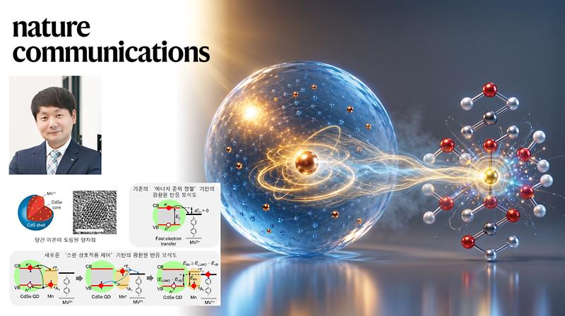
Abstract Spin-active dopants offer a powerful yet largely unexplored route for controlling interfacial redox chemistry in quantum-confined semiconductors. Here we show that manganese doping in cadmium selenide quantum dots enables an ultrafast spin-exchange-mediated electron-transfer pathway that allows methyl viologen reduction even when conventional band-edge energetics are unfavorable for charge transfer. Femtosecond transient absorption spectroscopy reveals that manganese dopants accelerate electron-transfer dynamics by more than an order of magnitude while opening a hot-exciton reduction channel in which a manganese ion captures a photoexcited exciton prior to phonon-assisted cooling. Subsequent spin-flip relaxation of the excited manganese ion drives charge separation and reduction of a molecular acceptor. This mechanism operates efficiently across resonant and off-resonant (energy-uphill and downhill) regimes, identifying spin-exchange coupling—rather than band alignment—as the dominant factor governing electron-transfer rates and efficiencies. These findings establish magnetic doping as a viable strategy for harvesting hot carriers and enabling energetically demanding photocatalytic transformations. For decades, researchers have understood electron transfer in photocalysis through one guiding principle. Electrons move most readily when the energy levels of a semiconductor and a reacting molecule are well matched. Researchers at UNIST and Los Alamos National Laboratory (LANL) have demonstrated that spin interactions can provide an alternative pathway, allowing electron transfer even when conventional energy-level alignment is unfavorable. Professor Ho Jin of the Department of Chemistry at UNIST, in collaboration with Dr. Victor I. Klimov of LANL, showed that manganese ions inside semiconductor quantum dots (QDs) create an ultrafast spin-exchange pathway that channels hot-electron energy into photoreduction reactions. The findings offer a new way to design photocatalysts that make better use of sunlight for hydrogen production and carbon dioxide conversion. QDs readily transfer photoexcited electrons to nearby molecules, making them attractive materials for photocatalysis. Their most energetic electrons, however, lose excess energy almost immediately, leaving little time for useful chemical reactions to occur. The team addressed this challenge by introducing magnetic manganese ions into cadmium selenide (CdSe) QDs. Before hot electrons could cool, the manganese ions captured their excess energy through ultrafast spin exchange. As the ions returned to their original spin state, that energy drove electrons into nearby molecules, triggering photoreduction reactions that would otherwise be difficult to achieve. Using femtosecond transient absorption spectroscopy, the researchers followed the electron transfer process in real time. Compared with undoped QDs, manganese-doped particles transferred electrons to methyl viologen more than ten times faster, demonstrating that spin exchange provides an efficient pathway for charge transfer. The team then asked whether the mechanism truly depended on hot-electron energy. When larger QDs were illuminated with higher-energy light, photoreduction readily occurred. Under lower-energy illumination, the reaction largely disappeared. Together, these experiments showed that manganese captures the excess energy of hot electrons before it is lost as heat. “We have traditionally thought of energy-level alignment as the deciding factor in electron transfer,” said Professor Jin. “Our results show that spin exchange can provide an alternative pathway, giving us a new way to harness the energy of hot electrons for photocatalysis.” Professor Ho Jin served as the first author of the study. Their findings were published in Nature Communications on June 26, 2026. Journal Reference Ho Jin, Valerio Pinchetti, Connor Orrison, et al., “Ultrafast photoreduction driven by interfacial spin exchange in manganese-doped quantum dots,” Nat. Commun., (2026).

2026.08.10

  • Chemistry
  • Department of Chemistry
  • Ho Jin
  • Hot Electron
  • Nature Communications
  • Quantum Dot
  • Spin Exchange)
  • Spin Relaxation

Smarter Design Method Improves Efficiency of In-Memory Computing Chips

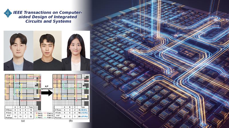
Abstract Data-centric applications continue to be limited by the memory wall. Logic-in-Memory (LiM) architectures based on non-volatile memories (NVMs), such as memristors, offer a promising solution by enabling in-memory computation and eliminating costly data movement. While several approaches leveraging memristor-aided logic (MAGIC) operations have been proposed, many fail to fully exploit the parallelism and spatial efficiency of memristor crossbars, especially under physical design constraints. In this paper, we propose a parallelism-driven, area-aware look-up table (LUT)-based mapping framework of arbitrary logic circuits into a memristor crossbar using MAGIC operations. We present a crossbar-aware floorplanning strategy that leverages topological LUT information to enable two-directional parallel computation (ie, HNOR and VNOR), thereby maximizing computational LUTs with minimal execution cycles. We formulate an integer linear programming (ILP) approach to define the placement of each LUT and its fanin locations, improving routability while preserving parallelism. Moreover, we introduce our novel A∗-search-based fan-in routing method with Hanan grid that fully utilizes the aligned fans and intermediate results. Experimental results demonstrate that the proposed framework achieves maximum parallelism and crossbar utilization, thereby reducing cycle counts by 19.6% and ensuring that all benchmarks map successfully under strict area constraints. We also confirm the scalability and practical applicability of the proposed framework for large-scale logic mapping in memristor-based LiM systems. Modern computing is increasingly limited not by processing speed, but by the time and energy required to move data between memory and processors. Researchers at UNIST have developed an automated design framework that addresses this challenge by making logic-in-memory (LiM) chips more efficient. Led by Professor Heechun Park of the Department of Electrical Engineering, the team designed a framework that automatically optimizes the placement of logic circuits and data pathways in memristor-based LiM architectures. By enabling more operations to run simultaneously while making better use of limited chip area, the approach reduced the number of computation cycles by nearly 20% compared with existing state-of-the-art methods. Unlike conventional computer chips, LiM architectures perform computation directly where data are stored, reducing costly data movement between memory and processors. This approach helps overcome the memory wall where data transfer limits overall computing performance. The framework determines where computations are performed within a memristor crossbar array and how intermediate results move to the next operation. Unlike previous approaches, it enables computations to proceed in both the horizontal and vertical directions, allowing more operations to run simultaneously while making better use of the available chip area. The framework also reorganizes intermediate data during computation, freeing unused memory cells and reducing wasted space. It then identifies efficient routes for transferring intermediate results between computational blocks, preserving parallel execution even under tight area constraints. In benchmark evaluations, chips designed using the new framework required 19.6% fewer computation cycles than those designed using existing approaches. The framework also successfully mapped every benchmark circuit, including designs that previous methods could not accommodate under the same area constraints, suggesting it can scale to larger LiM systems. “The performance of LiM computing depends not only on the memory device itself, but also on how computations are organized within the array,” said Professor Park. "By arranging operations to maximize parallel execution, our framework improves efficiency while remaning practical under realistic area constraints." The research was conducted by Ikkyum Kim and Minhong Kim as first and second authors, respectively, with Professor Heechun Park serving as the corresponding author. The findings were published online in IEEE Transactions on Computer-Aided Design of Integrated Circuits and Systems (IEEE TCAD) on June 2, 2026. The research was supported by the National Research Foundation of Korea (NRF) and the Institute of Information & Communications Technology Planning & Evaluation (IITP). The EDA tool was supported by the IC Design Education Center (IDEC). Journal Reference Ikkyum Kim, Minhong Kim, and Heechun Park, “A Parallelism-Driven, Area-Aware Technology Mapping Framework for Memristive Logic-in-Memory,” IEEE TCAD , (2026).

2026.08.06

  • AI Training
  • Department of Electrical Engineering
  • EE
  • Heechun Park
  • IEEE TCAD
  • Memory Wall
  • Memristive Logic-in-Memory
  • Non-volatile Memory
  • Parallelization
  • Technology Mapping

New Organic Photodetector Improves Polarized Near-Infrared Light Detection

Abstract Near-infrared (NIR) circularly polarized light (CPL) photodetection is of great importance due to its broad application potential in bioimaging, wearable healthcare, optical communication, and advanced optoelectronic systems. In this study, a supramolecular chirality evolution strategy in chiral low-bandgap fused-ring conjugated molecules (LFCs) is presented for high-performance NIR CPL photodetection using Schottky barrier vertical organic field-effect transistors (SB-VOFETs). Halogen substitution combined with thermal annealing drives inversion and amplification of supramolecular chirality in enantiopure LFC thin films. F-substituted LFCs exhibit progressive domain growth and hierarchical ordering with increasing annealing temperature, whereas Cl-substituted LFCs show limited structural evolution above 150°C. These distinct crystallization behaviors directly correlate with chiroptical responses, with F-substituted LFCs achieving a maximum absorption dissymmetry factor (|gabs|) of ∼0.1. When integrated into SB-VOFETs, the optimized chiral films enable highly efficient NIR CPL photodetection, delivering a photocurrent dissymmetry factor (|gph|) of ∼0.1, a specific detectivity of 4.9 × 10¹¹ Jones, an external quantum efficiency exceeding 900%, and a fast response time of ∼600 µs at 850 nm. These metrics represent the highest performance reported for NIR CPL. This study provides design guidelines for advancing high-performance chiral optoelectronic devices through the synergistic integration of atomic substitution, thermal annealing, and device architecture engineering. Near-infrared (NIR) circularly polarized light (CPL) carries information that conventional light cannot, making it valuable for applications ranging from autonomous vehicle sensors and bioimaging to optical security and advanced communications. Detecting this light accurately, however, has remained difficult because the organic semiconductor films used in these devices often lose the molecular order needed to distinguish different polarization states. A research team, led by Professor BongSoo Kim of the Department of Chemistry at UNIST and Professor Joon Hak Oh of Seoul National University has found a way to overcome that limitation. By controlling how chiral organic semiconductor molecules organize within thin films, the researchers significantly improved the films' ability to distinguish between left- and right-handed CPL. When incorporated into a photodetector, the optimized films delivered what the team reports as the highest performance yet achieved for NIR CPL detection. Unlike conventional light detectors, CPL can distinguish between two different polarization states of light. This additional information can reveal not only an object's shape but also properties, such as its surface composition or molecular structure, making the technology valuable for sensing and imaging applications. The researchers achieved the improvement by applying a simple thermal annealing process to thin films made from fluorine-substituted chiral organic semiconductor molecules. Rather than remaining randomly arranged, the molecules reorganized into larger, more ordered crystal domains. This more ordered molecular arrangement strengthened the film's interaction with CPL. As a result, the film's ability to selectively absorb CPL increased more than threefold after annealing at 250°C, with its absorption dissymmetry factor rising from approximately 0.03 to 0.1. Structural analysis confirmed that the annealed films adopted a highly ordered molecular arrangement closely resembling that of single crystals. The researchers also discovered an unexpected effect. As the molecular packing reorganized, the film reversed the polarization it preferentially absorbed, demonstrating that heat treatment could control not only the strength but also the handedness of the material's optical response. By comparison, similar films containing chlorine instead of fluorine showed little structural change above 150°C and exhibited lower polarization selectivity after annealing. To turn these improved optical properties into measurable electrical signals, the team integrated the optimized films into a vertical organic transistor. The device architecture efficiently collected and amplified charges generated by incoming light, allowing the detector to fully capitalize on the improved molecular organization. The resulting photodetector achieved a photocurrent dissymmetry factor of 0.1 at a wavelength of 850 nanometers, demonstrating excellent discrimination between left- and right-handed CPL. It also recorded a specific detectivity of 4.9 × 10¹¹ Jones, an external quantum efficiency of up to 909%, and a response time of less than 600 microseconds—the highest performance reported to date for NIR CPL detectors. “We found that simply controlling how the molecules organize within a thin film can dramatically improve how the materials respond to CPL,” the research team said. “We hope this strategy will help advance next-generation optical sensors and imaging technologies that rely on precise light detection.” Their findings were published online in Advanced Science on June 28, 2026. The research was supported by the National Research Foundation of Korea (NRF) and the Ministry of Science and ICT (MSIT). Journal Reference Jaeyong Ahn, Kwangmin Kim, Sangwook Lee, et al ., “Thermally Driven Supramolecular Chirality Evolution in Low-Bandgap Fused-Ring Conjugated Molecules for High-Performance NIR Circularly Polarized Light Detection,” Adv. Sci., (2026).

2026.08.05

  • Advanced Science
  • Bioimaging
  • BongSoo Kim
  • Chemistry
  • Chirality
  • CPL
  • Department of Chemistry
  • NIR
  • Optical Security

New Benchmark Reveals Limits in How AI Understands Hands

Abstract Understanding the fine-grained articulation of human hands is critical in high-stakes settings such as robot-assisted surgery, chip manufacturing, and AR/VR-based human-AI interaction. Despite achieving near-human performance on general vision-language benchmarks, current vision-language models (VLMs) struggle with fine-grained spatial reasoning, especially in interpreting complex and articulated hand poses. We introduce HandVQA, a large-scale diagnostic benchmark designed to evaluate VLMs' understanding of detailed hand anatomy through visual question answering. Built upon high-quality 3D hand datasets (FreiHAND, InterHand2.6M, FPHA), our benchmark includes over 1.6M controlled multiple-choice questions that probe spatial relationships between hand joints, such as angles, distances, and relative positions. We evaluate several state-of-the-art VLMs (LLaVA, DeepSeek and Qwen-VL) in both base and fine-tuned settings, using lightweight fine-tuning via LoRA. Our findings reveal systematic limitations in current models, including hallucinated finger parts, incorrect geometric interpretations, and poor generalization. HandVQA not only exposes these critical reasoning gaps but provides a validated path to improvement. We demonstrate that the 3D-grounded spatial knowledge learned from our benchmark transfers in a zero-shot setting, significantly improving accuracy of model on novel downstream tasks like hand gesture recognition (+10.33%) and hand-object interaction (+2.63%). Understanding a human hand gesture requires more than recognizing fingers. An AI model must also make sense of how those fingers bend, how joints related to one another, and how the entire hand changes with viewpoint. Current vision-language models remain surprisingly weak at this kind of finger-grained reasoning. A research team, led by Professor Seungryul Baek of the Graduate School of Artificial Intelligence at UNIST has developed HandVQA, a new benchmark that tests this ability in detail. Drawing on 3D hand data, the benchmark contains more than 1.6 million questions about joint angles, distances, and relative positions. It also gives researchers a way to improve the skills it is designed to measure. Despite strong performance on general image-and-language tasks, vision-language models can struggle when spatial differences become subtle. Existing benchmarks rarely examine hand anatomy at the level of individual joints, making these weaknesses difficult to measure. HandVQA fills that gap with questions generated from hand images and precise 3D joint coordinates. For each image, the benchmark asks 25 questions about properties such as finger flexion, the distance between joints, and whether one joint is above, below, in front of, or behind another. The results showed just how much current models miss. Without specialized training, several leading vision-language models performed near chance on some spatial questions and had particular difficulty judging distances between joints. They also made geometric errors and, in some cases, referred to finger parts that did not exist in the image. But the same benchmark that exposed these weaknesses also helped correct them. After LLaVA was fine-tuned with HandVQA, its accuracy on questions about joint distances increased from 16.20% to 90.79%. The benefits also carried over to tasks outside the benchmark. Qwen-VL, after learning from HandVQA, improved on two tasks it had not been directly trained for: hand gesture recognition by 10.33 percentage points and hand-object interaction by 2.63 percentage points. This transfer suggests that the model learned a broader understanding of hand geometry rather than simply becoming better at answering HandVQA questions. “HandVQA not only helped the model answer questions it had previously struggled with, but also improved its ability to handle new tasks,” said MD Khalequzzaman Chowdhury Sayem, first author of the study. “The spatial knowledge learned from the benchmark transferred to other hand-related tasks without requiring additional task-specific training.” Professor Baek added, “Accurately understanding hand pose is important in applications where even small errors can matter, from robotic manipulation and AR/VR interfaces to assistive technologies. HandVQA helps identify where current models fall short and provides a way to improve those capabilities.” Their findings have been accepted to the IEEE/CVF Conference on Computer Vision and Pattern Recognition (CVPR) 2026, one of the leading international conferences in computer vision. The study was supported by the National Research Foundation of Korea (NRF) through the Mid-Career Researcher Program and the Basic Science Research Program, along with programs administered by the Institute for Information communication Technology Planning and Evaluation (IITP), including the AI Star Fellowship, AI Graduate School, and the LG AI STAR Talent Development Program for Leading Large-Scale Generative AI Models in the Physical AI Domain programs. Journal Reference MD Khalequzzaman Chowdhury Sayem, Mubarrat Tajoar Chowdhury, et al. , “HandVQA: Diagnosing and Improving Fine-Grained Spatial Reasoning about Hands in Vision-Language Models,” CVPR '26, (2026).

2026.08.04

  • AIGS
  • AR
  • Computer Vision
  • CVPR
  • Graduate School of Artificial Intelligence
  • Hands
  • HandVQA
  • Pattern Recognition
  • Seungryul Baek
  • Vision-Language Models
  • VR

Solution-Processed Semiconductor Enables High-Performance RF Switches for 6G and Satellite Communications

Abstract Next-generation 6G communication requires radio-frequency components capable of operating above 100 GHz with low loss, high isolation, and zero static power—requirements that challenge complementary metal-oxide-semiconductor (CMOS) and microelectromechanical systems (MEMS) technologies. Here, we report transfer-free, large-area millimeter-wave (mmWave) switches based on solution-processed MoS2. While solution-processed 2D materials are often viewed as inferior to their crystalline counterparts due to high defect densities, we demonstrate that their edge-rich morphology is, in fact, a performance enabler. These edge defects act as intrinsic templates that confine Cu-filament pathways, enabling rapid (76 ns) and low-energy switching (1.57 nJ) with > 2000 cycles and uniform zero static-power operation, as corroborated by Kelvin probe force microscopy, conductive atomic force microscopy and low-temperature studies. The resulting switches achieve an low insertion loss ( < 0.1 dB) and high isolation ( > 35 dB) at 67 GHz. Notably, they exhibit a switching figure-of-merit (RON·COFF) of ~ 0.8 fs (fco ~ 187 THz), surpassing previously reported 2D switches. Importantly, by adopting an inverse-state operational scheme in a SHUNT architecture, we mitigate self-switching and achieve improved power handling (P0.1dB > 10 dBm) and linearity (IIP3 > 42.1 dBm). Finally, we demonstrate the platform's circuit-level viability by integrating the switches into a true-time-delay and hybrid-coupled phase shifters targeting 30 GHz mmWave applications. Researchers at UNIST have developed a high-performance radio-frequency (RF) switch using a solution-processed two-dimensional (2D) semiconductor, demonstrating stable operation at frequencies up to 67 GHz while consuming no static power. The technology could support future 6G wireless networks, satellite communications, radar systems, and other high-frequency communication platforms that demand compact, energy-efficient components. Led by Professor Myungsoo Kim of the Department of Electrical Engineering, the team fabricated the device using a thin film of solution-processed molybdenum disulfide (MoS2). Unlike conventional fabrication methods that require 2D semiconductor films to be grown and transferred onto a substrate, the new approach forms the semiconductor layer directly from a liquid precursor, simplifying manufacturing and making large-area production more practical. RF switches are fundamental components in wireless communication systems. They control the flow of high-frequency signals in smartphones, wireless base stations, satellite communications, radar systems, and autonomous vehicles. As communication technologies move toward the millimeter-wave frequencies required for future 6G and space communications, RF switches must transmit signals with minimal loss, effectively block unwanted leakage, and operate with very low power consumption. The newly developed switch achieved all three. Operating at 67 GHz, it recorded an insertion loss below 0.1 dB and signal isolation greater than 35 dB, allowing nearly all of the incoming signal to pass while suppressing signal leakage to less than 0.03%. The device also requires no standby power. Once switched on or off, it maintains its operating state even after power is removed, reducing unnecessary energy consumption. The researchers attribute the device's durability to the characteristics of the solution-processed MoS2 film. During fabrication, naturally occurring sulfur vacuums help guide the movement of copper ions that create the conductive pathways responsible for switching. Rather than reducing performance, these defects stabilize the switching process. Devices fabricated using solution-processed films continued to operate reliably after more than 2,000 switching cycles, whereas comparable devices fabricated from mechanically exfoliated MoS2 showed a lifetime of only about 100 cycles. To evaluate its practical potential, the team integrated the switch into communication circuits used for high-frequency signal control, including a transmit/receive switch and a beam-steering phase shifter. Both operated successfully, demonstrating that the technology can be incorporated into circuits used in satellite communications, radar, defense systems, and future wireless networks. Beam-steering phase shifters electronically direct radio waves without physically moving the antenna, enabling fast and precise tracking of moving targets such as satellites and drones. “By using solution-processed 2D semiconductor materials, we developed an RF switch that combines low signal loss with excellent isolation in the millimeter-wave band without requiring complex transfer processes,” said Professor Kim. “Because the switch retains its operating state even when power is removed, it consumes no standby power and could contribute to smaller, more energy-efficient communication systems for 6G, satellite communications, radar, and defense applications.” The findings were published online in Nature Communications on June 18, 2026. The research was supported by the National Research Foundation of Korea (NRF) and the Institute of Information & Communications Technology Planning & Evaluation (IITP), including the Space-K BIG Project and the InnoCORE Program of the Ministry of Science and ICT (MSIT). Journal Reference Changwoo Pyo, Sungmoon Park, Seungchan Lee, et al ., "Sub-femtosecond figure-of-merit millimeter-wave switches via solution-processed MoS2 for 6G radio-frequency front-ends," Nat. Commun ., (2026).

2026.08.03

  • 2D Materials
  • 6G
  • Department of Electrical Engineering
  • EE
  • MoS2
  • Myungsoo Kim
  • RF Switches
  • Satellite Communications
  • Semiconductor

Beyond the Obvious

《Editor's Note: The biggest scientific advances do not always come from discovering something new. Sometimes, they begin by seeing familiar problems in a new light. This month's stories invite us to look beyond the obvious. Across artificial intelligence, semiconductor materials, nanotechnology, and biomedical science, UNIST researchers examined assumptions, structures, and interactions that can easily go unnoticed—but often determine how a system behaves. Their findings show how a deeper understanding of what is already there can open new directions for discovery.》 Questioning Assumptions “The first answer is not always the right one.” Scientific discovery often begins by asking whether the original question was complete. Several AI studies featured this month did just that, revisiting assumptions about how machines learn, forget, reason, and communicate. In federated learning, researchers found that differences in camera viewpoints—not only privacy constraints or data distribution—can significantly affect how well AI models learn together. Another team showed that machine unlearning involves more than simply removing data: forgetting can unintentionally alter knowledge that should remain. Elsewhere, a new communication framework showed that effective cooperation among AI agents depends less on exchanging more information than on exchanging the right information. Other studies reconsidered how AI systems reason across multiple views of the same scene and explored how quantum computing could reduce the cost of training robust AI models. Different problems, but a common starting point: questioning the assumptions built into them. Together, these studies point to a simple lesson: better answers often begin with better questions. ■ Rethinking Federated Learning: Camera Viewpoints Matter (CVPR 2026) ■ Making AI Forget—Without Losing What Matters (ICML 2026 ) ■ Smarter Communication for Collaborative AI (ICML 2026) ■ Rethinking Multiview Reasoning (ICML 2026) ■ Quantum Algorithm Cuts the Cost of Training Robust AI (ICML 2026) Looking Beneath the Surface “The smallest details often hold the biggest clues.” Across materials science, biology, nanotechnology, and semiconductor engineering, UNIST researchers examined structures and interactions that are easy to miss but can have an outsized influence on how materials, devices, and biological systems behave. In semiconductor research, the spacing between neighboring atoms emerged as a critical factor in controlling material properties and device performance. At the nanoscale, researchers examined how the surface chemistry of quantum dots influences their behavior in imaging. Another study turned to microscopic wrinkles, showing how their geometry can reshape optical properties. The same attention to underlying mechanisms extended to biology, where researchers found that familiar forms of cell death do not always follow the pathways scientists expect. Together, these studies show how seemingly minor details—from atomic spacing and surface chemistry to microscopic geometry and cellular mechanisms—can fundamentally change our understanding of a system. Sometimes, the most consequential discoveries begin with something that was there all along, waiting to be examined more closely. ■ Atomic Precision for Better Semiconductors (Chem. Mater., 2026) ■ A New Perspective on QD Imaging (Nano Converg., 2026) ■ Wrinkles that Reshape Photonics (Adv. Funct. Mater., 2026) ■ When Cell Death Follows Different Rules (Cell Death Differ., 2026) Across very different fields, these studies share a common instinct: question the assumption, examine the detail, and look again. What appears familiar can still hold unanswered questions. Looking beyond the obvious is not simply how these discoveries were made. It is how scientific discovery moves forward. Explore the latest issue and follow 『The UNIST Brief』 on LinkedIn to stay updated. Subscribe via LinkedIn

2026.08.01

  • AI
  • AIGS
  • Atomic Precision
  • Bio
  • Cell Death
  • Collaborative AI
  • Department of Biological Sciences
  • DNA Curtain
  • ECE
  • ECHE
  • Federated Learning
  • Graduate School of Artificial Intelligence
  • Graduate School of Health Science and Technology
  • Graduate School of Semiconductor Materials and Devices Engineering
  • HST
  • LinkedIn
  • Machine Unlearning
  • Multiview Reasoning
  • MVProbe
  • Photonics
  • QRIM
  • Quantum Dots
  • Reinforcement Learning
  • School of Energy and Chemical Engineering
  • SE
  • Semiconductors
  • The UNIST Brief
  • Wrinkles

더보기

UNIST Insight

star

UNISTAR Voices 
Shaping Futures, 
Inspiring the 
World

더보기

Life at UNIST

star

더보기